Simulation and validation of transfer molding process of large-scale power semiconductor module
The transfer molding process is a widely used method for encapsulating microelectronics and power semiconductor devices. In power electronics, it is gaining increasing importance, particularly in the automotive sector [1]. In transfer molding, an epoxy mold compound (EMC) is injected under high pressure via the transfer pot and runner system into a mold, where it subsequently cures. At the beginning of the process, the EMC is in a solid, uncured state; during the process, it transitions into a liquid and begins to crosslink. Upon reaching a certain degree of cure, the material solidifies again.
This study presents a detailed COMSOL Multiphysics model of the complete transfer molding process, applied to a large-scale SiC power semiconductor module from Hitachi Energy. The model includes all essential stages of the process: preheating of the EMC, mold filling, curing, and final cooling to room temperature.
Preheating and mold filling were simulated using a non-isothermal, laminar two-phase flow model. The cure kinetics of the EMC were described using the Kamal equation [2] and implemented via a stabilized convection-diffusion equation, which was coupled to the flow through the velocity field. The non-Newtonian behavior of the liquid EMC was modeled using the Castro–Macosko approach [3]. To analyze mechanical stresses acting on the semiconductor module during injection, the entire filling process was coupled with a one-way fluid–structure interaction (FSI) model.
Based on the results of the filling simulation, two additional simulation steps were carried out to evaluate the mechanical loads on the module caused by volumetric shrinkage of the EMC during curing and subsequent cooling. In the mechanical step, the nonlinear viscoplastic material behavior was modeled using the Anand model [4].
The simulation results provide in-depth insights into the transfer molding process—both with regard to the flow behavior of the resin in the runner and mold, and the resulting mechanical stress state in the encapsulated semiconductor module.
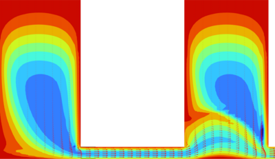
Key findings include: • Locally over-cured areas form in the runner system during filling, can lead to cross-sectional narrowing (Figure 1). • High bending stresses can arise in the module during the injection phase • The observed effects were experimentally confirmed and validated in the actual manufacturing process.
The results contribute to a better understanding of material behavior and stress development during transfer molding and can support further process improvements.

