Solder Degradation-based GaN Power Module Power Cycling Lifetime Prediction
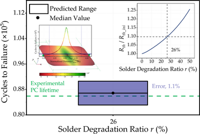
Gallium nitride (GaN) power modules are increasingly adopted in applications such as electric vehicle on-board chargers, due to their lower power loss and higher switching speed. To enhance power density and reduce parasitic inductance, modern packaging solutions are being developed toward eliminating bond wires and higher integration. Among them, the hybrid PCB-GaN-DBC structure stands out with a balance between efficiency and manufacturing maturity (Figure 1). However, its heterogeneous structure exacerbates thermomechanical vulnerability under coupled electrical, thermal, and mechanical loads due to coefficient of thermal expansion mismatches, making solder layers the most critical reliability risk in the packaging structure. To evaluate it, power cycling (PC) tests are commonly used, but direct monitoring of solder degradation in compact GaN packages remains impractical during the test process. This limitation creates significant demand for multiphysics simulation, which is dedicatedly solved in COMSOL Multiphysics, to analyze the relationship between solder degradation and PC lifetime, enabling more reliable package design. (Figure 2) This performed transient simulation involves: 1. Component Definition: A 3D geometric model matching actual dimensions was created in SolidWorks and imported into COMSOL. Material properties were assigned based on the physical module, with power loss defined as a temperature-dependent variable derived from LTspice device simulations. 2. Heat Transfer: The thermal solution incorporates convection boundary conditions at the bottom surface, computes temperature distribution by applying the characterized power loss to the GaN chip. 3. Solid Mechanics: Coupled with thermal results, the mechanical response is calculated using material constitutive models, including the Anand viscoplastic model for solder behavior. 4. Fatigue: The viscoplastic dissipation density of the solder layer across test cycles is captured and substituted into Morrow’s model to obtain the cycles to failure of the solder layer and derive the power module’s PC lifetime, by establishing a failure threshold for the solder degradation ratio based on power module’s thermal resistance increment (Figure 3). Enabled by COMSOL Multiphysics, during the simulation, the Lumped Thermal Network is implemented to efficiently simplify heat conduction between the GaN device and surrounding interconnection pads, with network parameters extracted from the precisely reconstructed device model. By importing OBD++ file, copper traces and vias on the PCB are modeled as zero-thickness thermal layers instead of their actual physical thickness in the geometric model. These two approaches collectively achieve over 20 times acceleration in computational speed. Furthermore, through model decomposition, the mesh quality of the solder layer is improved by a factor of 2.3, thereby ensuring accurate prediction of its mechanical response characteristics. The experimental validation shows the COMSOL simulation predicts the power module's PC lifetime within 1.1% error (Figure 4). Benefiting from the simulation approach, this work provides unique insights into solder behavior during PC tests that are unattainable through experimental measurements alone. It can then serve as an effective design tool for GaN packaging, enabling PC performance optimization while significantly reducing reliance on costly prototype fabrication and testing. Furthermore, its inherent multiphysics capability ensures adaptability to various boundary conditions and failure criteria, extending its applicability to broader power module reliability assessments.

